| client (0.6.2 anago only) | 2010-11-19 20:00 |
| kazzo (0.1.3) | 2010-03-13 00:09 |
Normally write waveforms are sent via the 60 pin edge connector. However occasionally this method causes three problems:
Read-access ROM area ($8000-$ffff) is assigned for reading ROM data, while the write-access ROM area is assigned as a control register for bank switching. But in order to program flash memory data, it requires sending a write-access signal. Due to this signal sharing the same function as bank switch control, certain steps must be taken in order to prevent such an accidental bank switch from occurring.
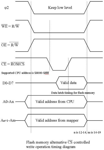
Flash memory has 3 control signals. They are CS (Chip Select), WE (Write Enable) and OE (Outout Enable). When these control signals are used, flash memory latches data.

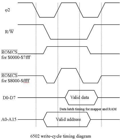
The 6502 has 2 control signals and 1 address-decoded signals: R/W (read or write), PHI2 (machine cycle), and /ROMCS (inverted (A15 and PHI2)). Many different mappers will latch data on the following condition:

The write cycle condition varies among different flash memory and mapper types. In order to successfully program data to flash memory, keep the PHI2 signal as a low state in order to prevent accidental bank switching.
When writing 0x2aaa, 0x5555 on address bus A0-14, flash memory will undesirably accept these writes as various other functions. Keep in mind that each bank switching specification amongst different devices will vary. In this case you will need to match the correct command addresses.
Please check out more info on command addresses in the accompanying Software Terminology document.
When using a basic board (which utilizes a 74xx161) the control signal for ROM is not fully decoded. This causes both the CPU and ROM to send data at the same time whenever the CPU sends a write waveform, which results in unusable data.
Normally this shouldn't pose a problem when using a ROM + 74xx161. However, it's a serious problem for both RAM and flash memory.
Many ASICs (e.g. MMC and VRC series) won't have such a databus conflicting problem. ASICs outputs a mixed signal, /OE and /CS, for ROM.
R/W CPU /ROMCS|memory /enable
L   L         |H
L   H         |H
H   L         |L
H   H         |H
Address bus and data bus is same connection for ROM. Connect GND or +5V to the higher address bus that is INDEPENDENT from the mapper logic.
/CS requires address decoded parts. Connect to /ROMCS. Otherwise if $6000-$7fff is assigned for ROM, the flash process will not work.
Connect to R/W.
/OE requires a high state while R/W is at low state. This normally shouldn't matter with ASICs since it outputs a mixed signal. Otherwise if the mixed signal is not available, connect /OE to the inverted R/W instead.
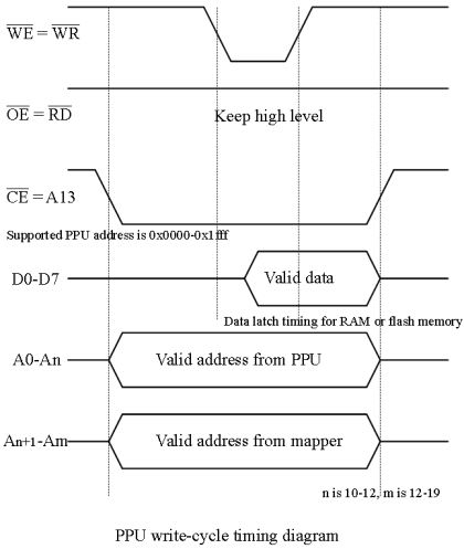
Address bus and databus connection share the same CPU region. But since the PPU control signals are much simpler than CPU signals, there's no issues with accidental bank switching. Connect following assingment.
Notes:

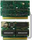
Sample picture for HVC-TKROM (60pin connector, MMC3, Program ROM, Charcter ROM and Battery-backuped W-RAM)

 You need to bend the leg #31 in CHR memory and legs #30 and #31 in PRG memory.
Pictures were provided by Mike. (Thanks!)